At its 2023 North American Innovation Seminar today, TSMC has actually divulged extra information about its prepare for its upcoming N2 2nm-class production nodes in 2025– 2026 and beyond. TSMC’s N2 household of fabrication innovations will be broadening with extra variations, consisting of N2P with behind power shipment, and N2X for high-performance computing. In between these upcoming N2 generation procedure nodes, TSMC is setting out a roadmap to continue their unrelenting speed of increasing transistor performance effectiveness, enhance power usage, and enhancing transistor density.
N2 Gets Denser
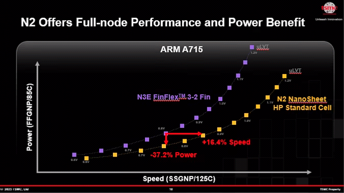
TSMC’s preliminary N2 production procedure, which was presented in 2015, will be the foundry’s very first node to utilize gate-all-around (GAAFET) transistors, which TSMC is calling Nanosheet transistors. GAAFET’s benefits over present FinFET transistors consists of decreased leak present (as gates exist on all 4 sides of the channel), in addition to the capability to change channel width for greater efficiency or lower power usage.
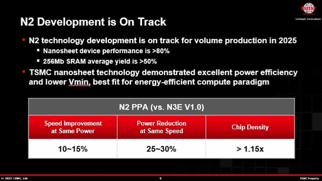
When presenting this innovation in 2015, TSMC stated that it would improve transistor efficiency by 10% to 15% with the exact same power and intricacy, or lower power usage by 25% to 30% at the exact same clock and transistor count. The business likewise states that N2 will provide ‘blended’ chip densities of over 15% higher than N3E, which is a boost from the 10% density boost revealed in 2015.
Today, the business stated that N2 innovation advancement is on track and the node will get in high-volume production in 2025 (most likely really late 2025). The business likewise stated that its Nanosheet GAA transistor efficiency is attaining much better than 80% of its target specs 2 years prior to getting in HVM, which typical yield of a 256Mb SRAM test IC is over 50%.
” TSMC nanosheet innovation showed outstanding power effectiveness and lower Vmin, finest suitable for energy-efficient calculate paradigm,” a declaration by TSMC checks out.
| Promoted PPA Improvements of New Process Technologies . Information revealed throughout teleconference, occasions, press rundowns and news release |
|||||
| TSMC | |||||
|
N5 . vs . N7 |
N3 . vs . N5 |
N3E . vs . N5 |
N2 . vs . N3E |
||
| Power | >-30% | -25 -30% | -34% | -25 -30% | |
| Efficiency(* ) . | . | . | . | . | |
| .(* )? | ? | .(* )> 1.15 X(* ) . | Volume | . | |
| Q2/Q3 2023 .(* )H2 2025(* ) . |
* Chip density released by TSMC shows’ blended ‘chip density including 50 % reasoning, 30 % SRAM, and 20 % analog.(* )N2P Gets Behind Power Shipment In 2026 | Behind power shipment | Behind power shipment is development whose significance is tough to overemphasize. Chipmakers have actually been combating resistances in chip power shipment circuitry for many years, and behind power shipment networks (PDN) are a yet another approach to resolve them. In addition, decoupling PDN and information connections likewise aids with location decrease, so anticipate N2P to more boost transistor density compared to N2. | TSMC states that N2P is on track to be production all set in 2026, so we can hypothesize that the very first N2P-based chips will be offered in 2027. This timeline would put TSMC approximately 2 years behind competing Intel when it pertains to behind power, presuming they have the ability to deliver their own 20A procedure on time in 2024. | |