At next week’s yearly VLSI Seminar, Intel will exist a trio of highly-anticipated documents about their development with their upcoming PowerVia chip fabrication innovation– the business’s in-development application of behind power shipment networks. Together with Intel’s RibbonFET innovation for gate-all-around transistors, PowerVia and RibbonFET are slated to act as Intel’s huge one-two punch to the remainder of the silicon lithography market, presenting 2 significant chip innovations together that Intel thinks will rise them back into the fabulous management position. Integrated, the 2 innovations are going to be the foundation of Intel’s “angstrom” period fab nodes, which will enter into high volume producing next year, making Intel’s development with the brand-new innovations a topic of excellent significance both inside and beyond the business– and one which Intel wishes to attend to.
When it concerns Intel’s chip production innovation, the stakes for Intel’s R&D groups could not be any greater than they are right now. The veteran leader of the fab would has faulted– consistently– and is now in the middle of a multi-year effort to course-correct, not just to return that management position which they have actually lost, however to get into the agreement chip production service in a huge method.
As an outcome, while VLSI research study documents do not typically draw in a lots of outdoors attention, this year in specific is a huge exception. With RibbonFET and PowerVia set to enter into production next year, Intel is reaching the point where they’re concluding R&D deal with the very first generation of those innovations. Intel is now at the point where, to their peers in the VLSI market, they can provide their very first findings around producing an intricate reasoning test chip. And to Intel’s financiers and other outsiders, Intel can reveal the very first genuine proof that their efforts to return on track might effectively be prospering, providing Intel an opening to jump ahead of the competitors that the business considerably requires.
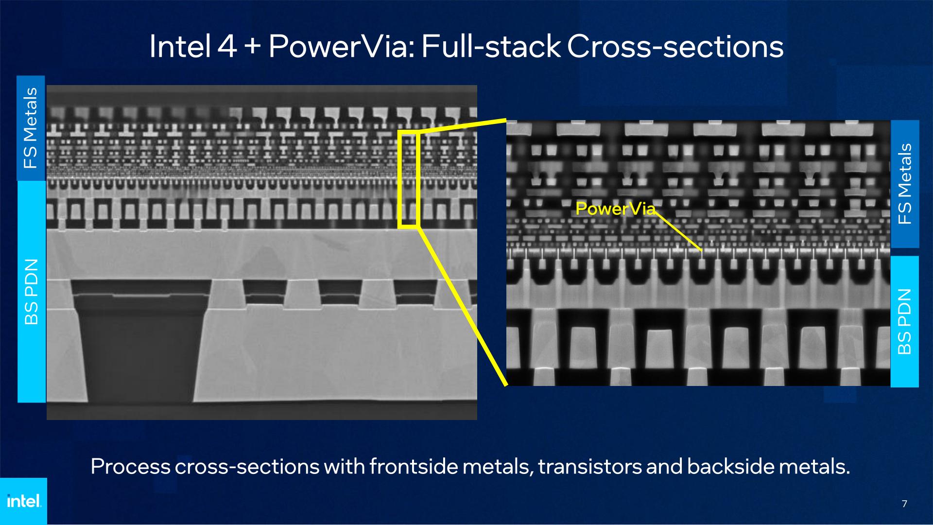
To that end, at next week’s seminar Intel is going to be revealing a good deal of info around their application of behind power shipment network innovation, which they call PowerVia. Central to these documents is Blue Sky Creek, an Intel “product-like” reasoning test chip that carries out behind power shipment on the EUV-enabled Intel 4 procedure innovation. With Blue Sky Creek, Intel plans to show that not just do they have PowerVia dealing with a CPU on time for high volume producing next year, however that the efficiency and production advantages of behind power shipment are whatever Intel has actually assured. Suffice it to state, Intel is getting ready for this year’s VLSI conference to be a huge minute for the business.
Backgrounder: Behind Power Shipment
Behind power shipment networks (BSP/BS-PDN) is an innovation principle that has actually been silently in advancement for the previous numerous years throughout the whole chip fab market. Comparable to EUV in current fab nodes, BS-PDN is viewed as a necessary innovation to continue establishing ever-finer procedure node innovations, and as an outcome, it’s anticipated that all leading-edge chip fabs will relocate to the innovation in the future.
With that stated, they are not all moving there at the very same time. Intel anticipates to be very first of the huge 3 chip fabs to productize the innovation, bringing it into chips a minimum of 2 years ahead of its rivals. As an outcome, Intel is quite the pathfinder for the innovation, which includes no scarcity of dangers– however it likewise includes considerable benefits for getting the innovation (and their timing) appropriate. For Intel, the business thinks that this will be their brand-new FinFET minute– a recommendation to Intel’s intro of FinFETs on 22nm in 2012, which sealed Intel’s lead in the market for numerous years. This is especially essential as Intel will not have a lead over its rivals when it concerns gate-all-around FETs (GAAFET) timing, so BS-PDN/PowerVia is going to be Intel’s trump card in the fabulous area for the next couple of years.
On the other hand, to completely comprehend how BS-PDN works, the very best location to begin is to evaluate how standard (frontside) power shipment works, so that we can contrast that to the lots of modifications that feature constructing a BS-PDN wafer.
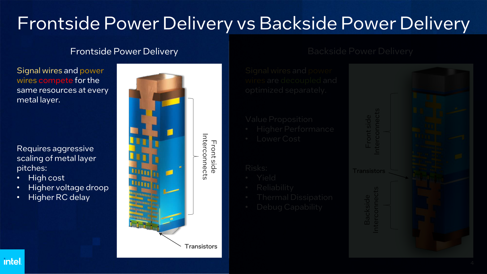
The production procedure of a modern-day, frontside power shipment chip begins with engraving the transistor layer, M0. This is the tiniest and most elaborate layer on a die, and is where high-precision tools like EUV and multi-patterning are required one of the most. Simply put, it’s the most pricey and intricate layer of the chip, which has considerable implications for both how chips are built and how they are evaluated.
Above that, extra metal layers are included at increasing sizes to represent all the electrical wiring required in between the transistors and various parts of the processor (cache, buffers, accelerators), in addition to supplying routing for power that is available in from even further up the stack. Intel compares this comparable to constructing a pizza, which is an unrefined example, however reliable.
A modern-day high-performance processor generally has anywhere from 10 to 20 metal layers in its style. With the Intel 4 procedure in specific, there are 16 layers for reasoning, varying from a pitch of 30 nm approximately 280 nm. And after that there’s another 2 “huge metal” layers on top of that simply for power routing and positioning external adapters.
As soon as a die has actually been completely fabbed and polished, the die is then turned over (making this a flip chip) so that the chip can speak to the outdoors world. This flip locations all the adapters (power and information) at the now-bottom of the chip, while the transistors wind up at the top of the chip. As soon as flip chip production was mastered, this made chip debugging and cooling specifically hassle-free, as it enabled debugging tools simple access to the critical transistor layer. On the other hand those hot little gates likewise ended up being specifically near to the chip’s cooler, enabling the reasonably simple transfer of heat out and away from a chip.
The downside with frontside power shipment, nevertheless, is that it implies both power and signal wires are on the very same side of the chip. Both wires need to take a considerable journey down through 15+ layers to reach the transistors, all the while contending for important area and producing disturbance with each other. For the power wires in specific, this is specifically a problem, as the resistance along these wires triggers the voltage of the inbound power to drop, which is referred to as the IR Drop/Droop result.
For the majority of the history of chip fabbing, this hasn’t been a substantial problem. However thus lots of other elements of chip structure, the issue has actually ended up being a growing number of noticable as chip function sizes have actually diminished. There is no apparent tough limitation here on frontside power shipment, however offered just how much more difficult it is to diminish chips with every succeeding generation, the issue has actually ended up being too huge (or rather, too pricey) to work around.
Which brings us to behind power shipment. If having both signals and power being available in on the very same side of the chip is triggering issues, why not separate the 2? This, in a nutshell, is precisely what behind power shipment seeks to solve, by moving all of the power connections to the opposite of the wafer.
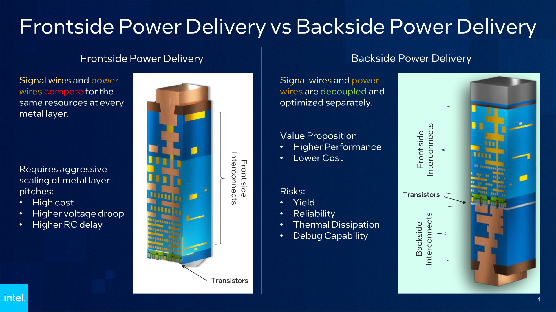
For Intel’s PowerVia application of this principle, Intel rather actually turns a wafer upside down, and polishes away practically all of the staying silicon till they reach the bottom of the transistor layer. At that point, Intel then constructs the metal layers for power shipment on the opposite side of the chip, comparable to how they would have formerly developed them on the front side of the chip. The net outcome is that Intel winds up with what’s basically a double-sided chip, with power shipment on one side and signaling on the other.
On paper (and in Intel’s paper), there are eventually numerous advantages to relocating to BS-PDN. Primarily, this has a significant effect on streamlining the building of a chip. We’ll get to Intel’s particular claims and findings in a bit, however of specific note here is that it enabled Intel to unwind the density of their M0 metal layer. Instead of needing a 30 nm pitch on Intel 4, Intel’s test node for Intel 4 + PowerVia enabled a 36 nm pitch. That straight streamlines the most intricate and pricey processing action of the whole chip, rolling it back to something better in size to the Intel 7 procedure.
BS-PDN is likewise primed to provide some modest efficiency enhancements to chips also. Reducing the path for power shipment to the transistors with something more direct assists to combat the IR Droop result, leading to much better power shipment to the transistor layer. And getting all of those power shipment wires out of the signal layers enhances the efficiency of those also, getting rid of the power disturbance and providing chip designers more space to enhance their styles.
Otherwise, the compromise for all of this is mostly in losing the formerly pointed out benefits of constructing a frontside chip. The transistor layer is now approximately in the middle of the chip, instead of at the end. This implies that standard debugging tools can’t straight poke the transistor layer of a finished chip to evaluate it, and there is now 15 approximately layers of signal wires in between the transistor layer and the cooling service. These aren’t overwhelming obstacles, as Intel’s paper makes sure to set out, however were problems that Intel needed to work around in their style.
Manufacturability is the other set of compromises associated with relocating to BS-PDN. Structure power layers on the behind of a die is something that’s never ever been done in the past, which increases the possibility of something failing. So not just does power shipment require to work, however it requires to work without substantially decreasing chip yields or otherwise making chips less trusted. However if all of these things turn out, then the additional effort of constructing power layers on the behind of a wafer are more than counteracted by the time and expense savings of not needing to path power in through the front side.
Intel’s Added Wrinkles: Provider Wafers & & Nano TSVs
Due to the fact that behind power shipment networks are going to end up being a market basic function in due time, we have actually attempted not to focus excessive on Intel’s particular application of BS-PDN/PowerVia. Today that we have actually struck the principles of BS-PDN, there are a number of Intel-specific application information worth keeping in mind.
Primarily, Intel is utilizing a provider wafer as part of their building procedure in order to offer chip rigidness. Bonded to the front side of a PowerVia wafer after the fabrication of that side is finished, the provider wafer is a dummy wafer to assist support the chip while Intel is blasting away at the opposite. Due to the fact that the two-sided chipmaking procedure polishes away a lot of the staying silicon wafer, there isn’t much structural silicon to hold the entire thing together. As Intel gently jokes, regardless of this being silicon lithography, there’s just a small quantity of silicon left on the wafer by the end.
That provider wafer, in turn, stays as part of the chip for the rest of its life. As soon as chip fabbing is finished, Intel can polish the bonded provider wafer to the essential density. Of note, since the provider wafer is on the signal side of the chip, this implies it provides another layer of product in between the transistors and the cooler. Intel’s strategies to enhance heat transfer take this into account, however for PC lovers accustomed to transistors at the top of their chip, this is going to be a considerable modification.
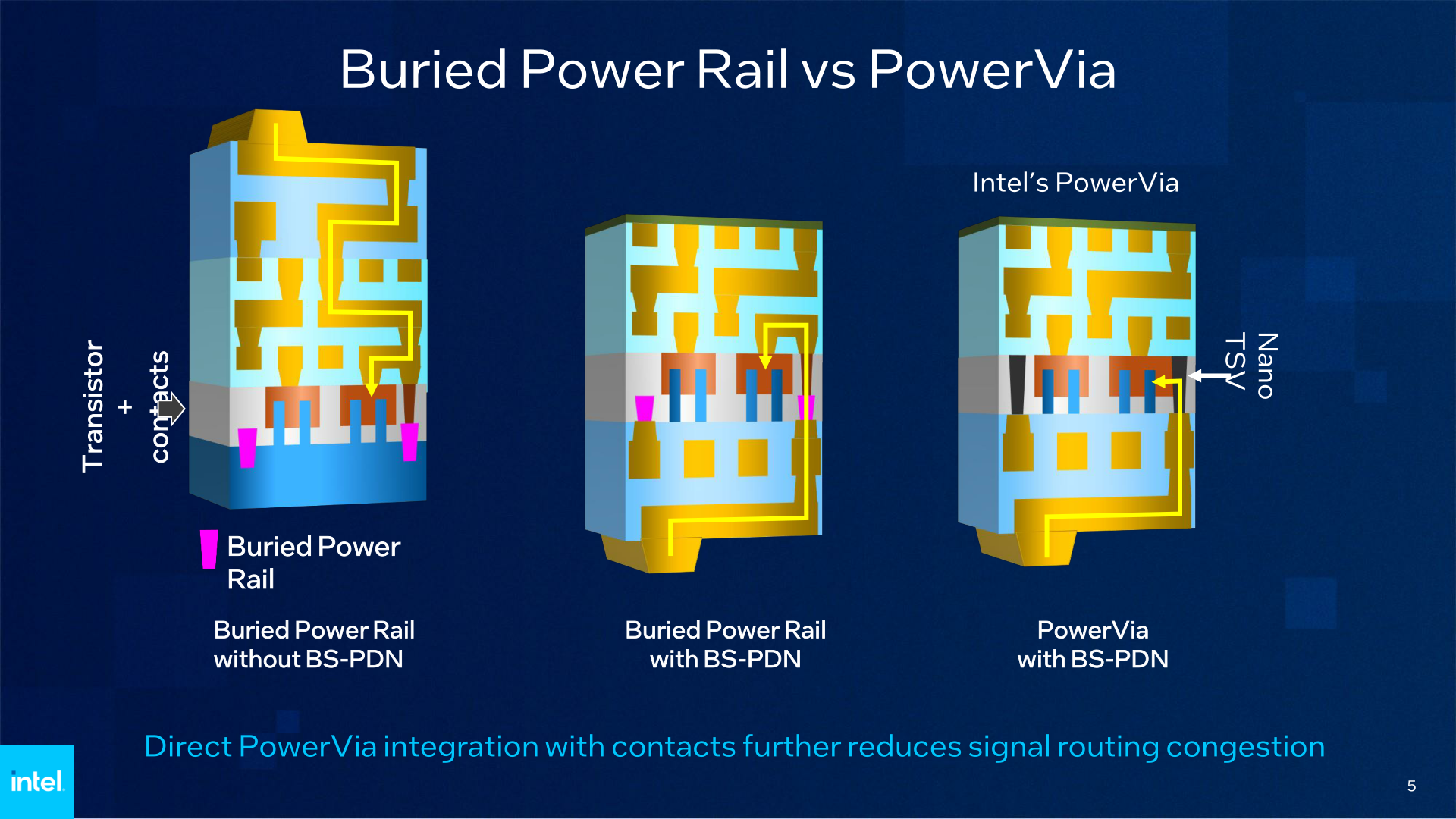
Intel’s other significant information with their application of BS-PDNs is using TSVs for power routing. In PowerVia, there are nano-scale TSVs (appropriately called Nano TSVs) in the transistor layer of the chip. This remains in contrast to buried power rails, which is what market leader IMEC has actually been checking out with their BS-PDNs.
The long and except matters is that while power rails still needed going up-and-over the transistor layer to provide power, using TSVs enables power to be provided more straight to the transistor layer. For Intel this is a technological benefit that they’re eager to make use of, as it prevents needing to style and build-in the routing needed for buried power rails.