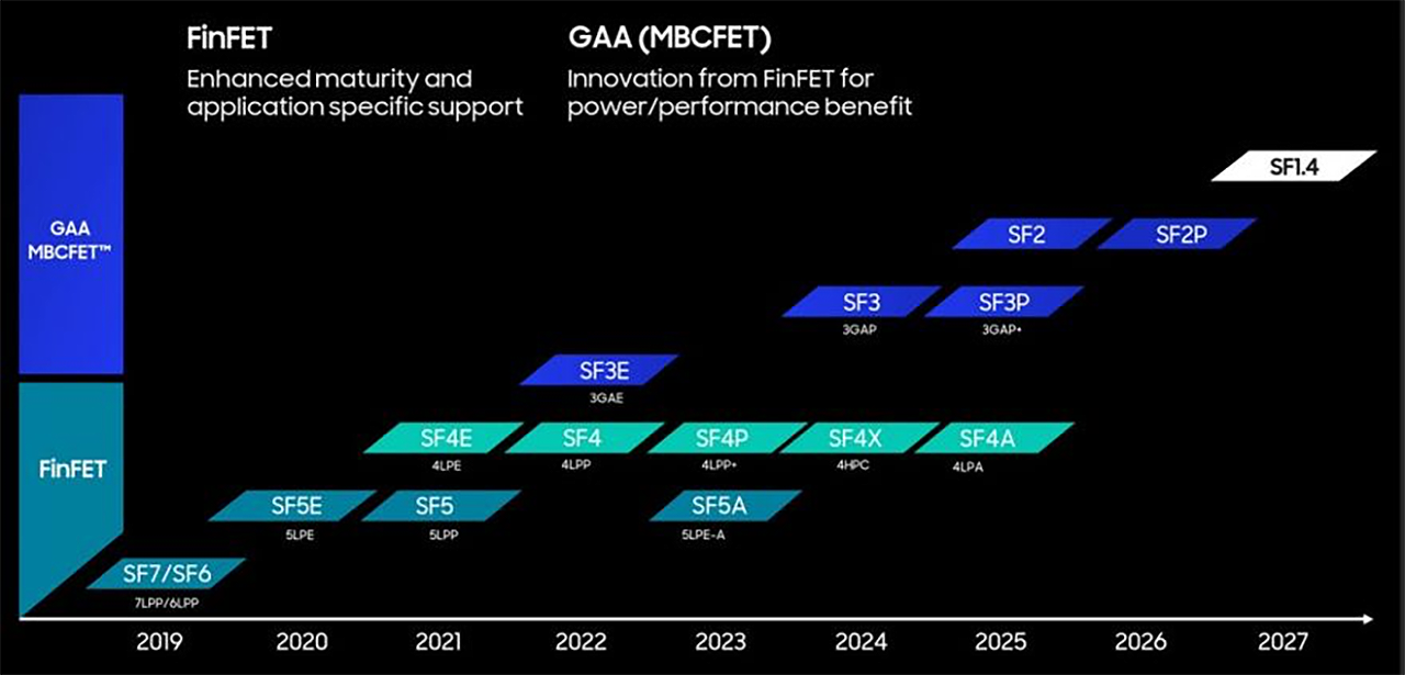
Presently, just 2 foundries provide their consumers 3 nm and 4 nm-class procedure innovations: TSMC and Samsung Foundry. However company media in some cases blames Samsung Foundry for average yields on leading-edge nodes, which can not be confirmed. However a set of current reports declare that Samsung is now at a point where they are delivering their very first GAAFET-based 3 nm chips to business consumers, which the yields of Samsung’s 3 nm and 4 nm-class nodes remain in good shape in general.
Samsung Foundry’s 4 nm-class procedure innovation yield is now greater than 75%. On the other hand, yields of chips on SF3E (3nm-class, gate-all-around early) now surpasses 60%, according to price quotes in a report from Hello there Financial investment & & Securities, a member of DGB Financial Group, reports Kmib.co.kr The very same report declares that TSMC’s yields at its N4 node technique 80%, however once again, this is a quote by a scientist.
In basic, info about yields at foundries can not be confirmed considering that agreement fabs practically never ever openly discuss yields. They in some cases divulge flaw density openly compared to previous nodes, however this is barely the case for Samsung Foundry’s SF4E, SF4, SF4P, and SF3E.
Formally, Samsung Foundry just states that its SF3E procedure innovation remains in high-volume production with steady yields (perhaps to deal with a media report from late in 2015 which stated that SF’s yields on SF3E were unsteady), and the advancement of refined SF3 is continuous.
“ We are standardizing the first gen 3nm procedure with steady yields, and, based upon this experience, we are establishing the second gen procedure to protect even higher mass production abilities,” a declaration by Samsung checks out.
On The Other Hand, TechInsights discovered among the very first chips made on Samsung’s SF3E procedure. This is the Whatsminer M56S++ which is obviously a cryptocurrency mining chip from MicroBT, a Chinese designer. Mining chips are reasonably simplified gadgets with loads of routine structures and couple of SRAM bit cells. Such chips are simple to construct and produce terrific pipeline cleaners for the most recent procedure innovations, so it is not unexpected that Samsung Foundry is making them instead of big ASICs on its SF3E. Though as a tip, smaller sized chips have inherently greater yield rates than big ASICs (lower chances of any provided chip covering a problematic area on a wafer), so the business practicality of the Whatsminer M56S++ does not indicate that a fairly big smart device or PC SoC would strike the very same yields or be similarly as feasible at this time.
There is an indirect verification that yields of Samsung’s 5 nm and 7 nm-class fabrication procedures are enhancing. The usage rate of Samsung Foundry’s for 5 nm-capable lines increased to 80%, and the combined usage rate of 5nm and 7 nm-capable fabs reached 90% just recently, up from 60% in 2022, according to a DigiTimes story that points out ET News Once again, the info originates from an informal source.
Generally, fabless chip designers are not inclined to utilize nodes with high flaw densities, so if the usage rate of 5 nm-class (Samsung’s SF4 stemmed from SF5) gets greater, this might show that they are now more intensively utilized by Samsung’s consumers. Additionally, this might be an indication that Samsung Foundry has consumers desperate enough to increase production regardless of low yields due to high need. Yet, provided the present market conditions, this might not hold true.
Sources: Kmib.co.kr, DigiTimes, TechInsights