Samsung has actually revealed this night that they have actually finished advancement on their very first generation of GDDR7 memory. The next version of the high bandwidth memory innovation, which has actually been under industry-wide advancement, is anticipated to strike the marketplace in 2024, with Samsung in prime position to be among the very first memory suppliers out of eviction. With their very first generation of GDDR7 parts slated to strike up to 32Gbps/pin of bandwidth– 33% more than their finest GDDR6 parts today– the business is aiming to provide a large boost in GDDR memory bandwidth on the back of the innovation’s adoption of PAM-3 signaling.
Samsung’s statement comes as we have actually been seeing a boost in disclosures and statements around the next version of the widely-used memory innovation. While a completed spec for the memory has yet to be launched by JEDEC, Samsung competitor Micron has actually formerly revealed that it prepares to present its own GDDR7 memory in 2024— a comparable timeline regarding Samsung’s existing schedule. On the other hand, EDA tool company Cadence divulged a substantial quantity of technical information previously this year as part of revealing their GDDR7 confirmation tools, exposing that the memory would utilize PAM-3 signaling and reach information rates of approximately 36Gbps/pin
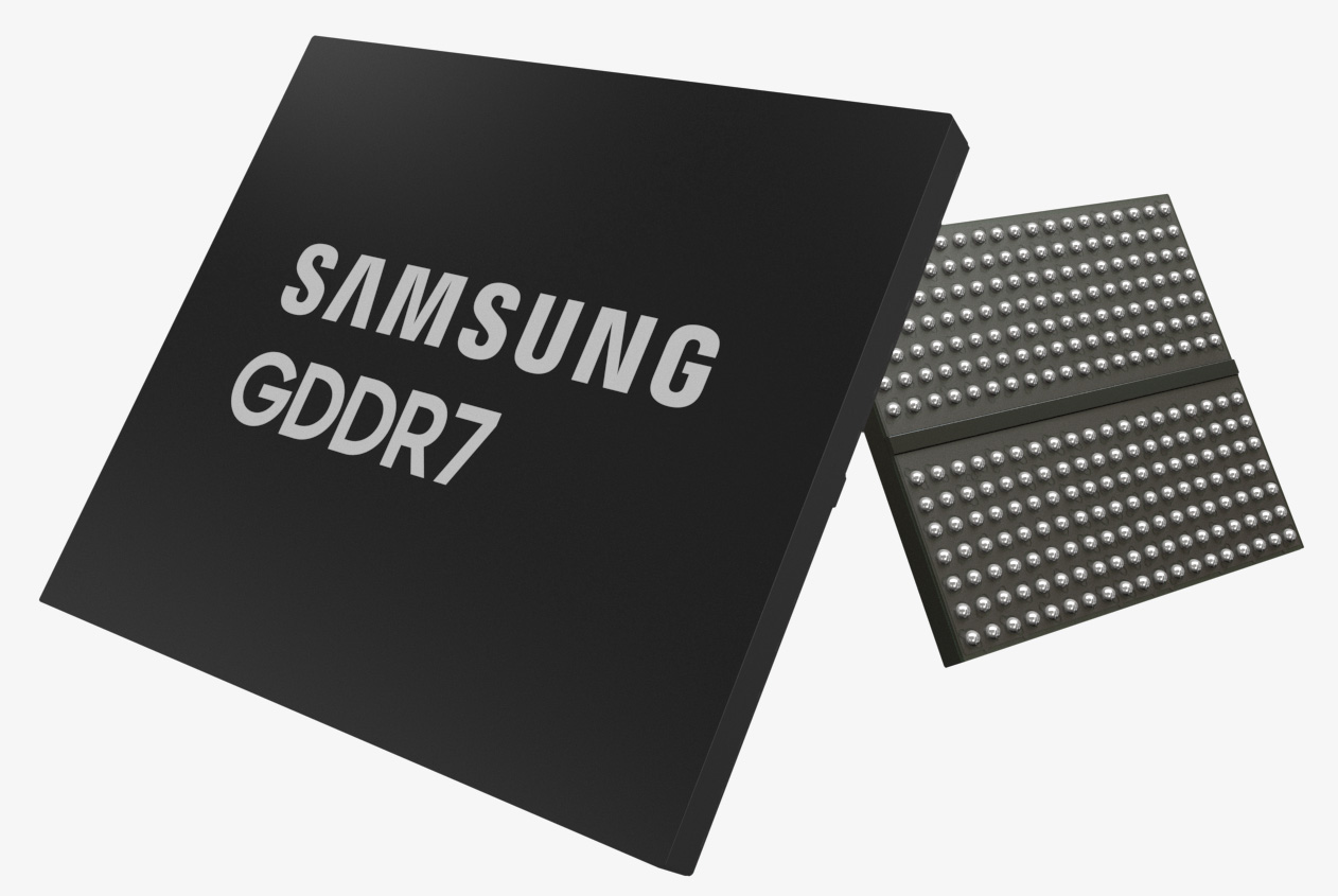
With today’s statement, Samsung has actually ended up being the very first of the significant memory producers to openly reveal that they have actually finished advancement of their very first generation of GDDR7. And while the business tends to make these sorts of memory statements fairly early in the bring-up procedure– well prior to memory is all set for business mass item– it’s none the less a crucial turning point in the advancement of GDDR7, as it suggests that memory and gadget producers can start recognition work versus practical hardware. When it comes to Samsung itself, the statement provides the Korean corporation a really noticeable chance to enhance their claim of management within the GDDR memory market.
Besides providing an upgrade on the advancement procedure for GDDR7, Samsung’s statement likewise offers some top-level technical information about the business’s very first generation of GDDR7– though “top-level” is the personnel word as this is not by any suggests a technical deep dive.
| GPU Memory Mathematics | |||||
| GDDR7 | GDDR6X | GDDR6 | |||
| B/W Per Pin | 32 Gbps( Predicted) | 24 Gbps( Shipping) | 24 Gbps( Testing) | ||
| Chip Density |
2 GB( 16 Gb) |
2 GB( 16 Gb) |
2 GB( 16 Gb) |
||
| Overall B/W( 256-bit bus) | 1024 GB/sec | 768 GB/ssec | 768 GB/ssec | ||
| . | .(* )1.35 V | 1.35 V | . | ||
| QDR | . | . | . | ||
| . | . | . | . | ||
| . | . | Surprisingly, this is beginning much closer to predicted limitations of GDDR7 than we have actually seen in previous generations of the memory innovation. Whereas GDDR6 gone for 14Gbps and ultimately scaled approximately 24Gbps, Samsung wishes to begin at 32Gbps. At the very same time, nevertheless, GDDR7 is going to be a smaller sized generational leap than we saw for GDDR6 or GDDR5; instead of doubling the signaling bandwidth of the memory innovation over its predecessor, GDDR7 is just a 50% boost, owing to the switch from NRZ (2 state) signaling to | (3 state) signaling. | ||
Update (7/19, 3pm ET):
Following a round of Q&A, Samsung has actually supplied some extra technical information on their first-generation GDDR7 memory, consisting of voltages (1.2 v), how they are determining energy effectiveness, and the procedure node being utilized (D1z). The remainder of the short article has actually been upgraded appropriately. At a high level, the bright side is that Samsung’s GDDR7 is slated to provide a concrete boost in energy effectiveness. With a small voltage of 1.2 v, GDDR7 needs less voltage to drive it than its predecessor. However with just a 20% total enhancement in energy effectiveness for a memory innovation that is providing up to 33% more bandwidth, this suggests that the outright power usage of the memory is increasing versus the previous generation
As Samsung’s energy effectiveness figures are for GDDR7@32Gbps versus GDDR6@24Gbps, we’re taking a look at around a 7% boost in overall energy usage. Which, luckily, is not a big boost in power usage. However it is a boost none the less.
Broadly speaking, this is the very same result as we saw with the intro of GDDR6( X), where regardless of the energy effectiveness gains there, total power usage increased from one generation to the next, as energy effectiveness gains are not equaling bandwidth needs. Not to state that any of this is unanticipated, however it suggests that excellent cooling will be a lot more important for GDDR7 memory.
However for customers with stringent power/cooling requirements, Samsung is likewise revealing that they will be making a low-voltage variation of their GDDR7 memory offered. This will be a 1.1 v variation of their GDDR7 chips, and while clockspeeds have not been divulged, we ‘d anticipate something closer to their GDDR6 clockspeeds. With current-generation GDDR6, high-end laptop computers are usually coupled with low-voltage memory running no faster than 18Gbps, so low-voltage GDDR7 performing at around 24Gbps would still represent a substantial advance.
Samsung has actually likewise validated that they’re going to be utilizing their D1z memory fab procedure for their very first generation GDDR7. This is the very same EUV-based procedure the business is utilizing for their latest GDDR6– however strangely enough, it’s older than the 12nm procedure Samsung exposed they’ll be utilizing in other places in a current DDR5 memory statement
The truth that the business isn’t utilizing a more recent node here is a bit unexpected, however from an architectural point of view, it likewise suggests that Samsung has actually attained a 20% boost in energy effectiveness without a more recent node. Architecturally-driven energy gains are rare in both the memory and reasoning areas nowadays, all of that makes for an appealing indication for the future of GDDR7.
Mentioning architecture and style, the business keeps in mind that their GDDR7 memory uses “IC architecture optimization” to keep power and heat generation in check. Though at this moment we do not have any additional information on simply what that suggests.
Electronic devices production aside, the last significant development with Samsung’s GDDR7 will be distinctly physical: epoxy. Plainly conscious of the currently high heat loads created by existing GDDR memory clocked at its greatest speeds, Samsung’s news release keeps in mind that they’re utilizing a brand-new epoxy molding substance (EMC) for GDDR7, which is developed to much better transfer heat. All informed, Samsung is declaring a 70% decrease in thermal resistance versus their GDDR6 memory, which ought to assist make sure that a great cooler can still pull enough heat from the memory chips, regardless of the total boost in heat generation.
Covering things up, now that preliminary advancement on their GDDR7 memory has actually been finished, Samsung is proceeding to confirmation screening with their partners. According to the business, they’ll be dealing with crucial consumers on confirmation this year; however at this moment, the business isn’t stating when they anticipate to start mass production of the brand-new memory. Offered the timing of Samsung’s statement (along with Micron’s), the preliminary market for GDDR7 appears to be AI and networking accelerators, instead of the video cards that GDDR7 gets its name from. With both AMD and NVIDIA hardly a quarter of the method through their existing architectural release cycles, neither business is most likely remain in a position to utilize GDDR7 in 2024 when it’s all set. Rather, it’s going to be the other users of GDDR memory such as networking items and high-performance accelerators that are most likely to be very first to utilize the innovation.